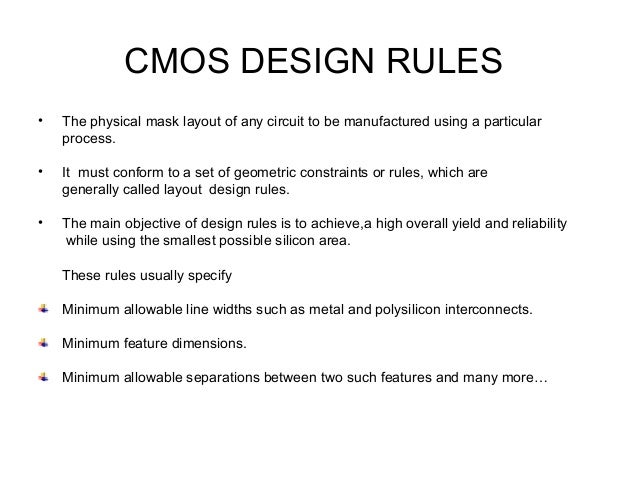
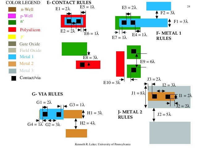
Mask Layout Design Rules

Layout Rules

Electronic Systems 2015 Cmos Design Rules Youtube
Layout Rules
Cmos Design Rule
Design Rules
Layout Stick Diagram Design Rules

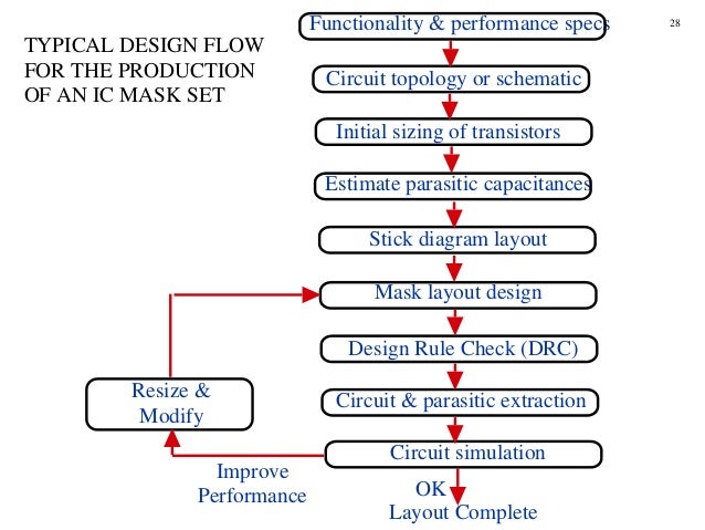
The physical mask layout design of cmos logic gates is an iterative process which starts with the circuit topology and the initial sizing of the transistors.
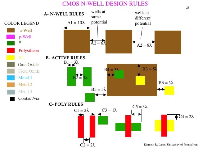
Mask layout design rules. Intra layer that is within one layer width spacing inter layer that is layer to layer spacing enclosure extension overlap rules are going to be separated into the masks. 2 design rules cmos vlsi design slide 3 layout overview minimum dimensions of mask features determine. Microfabrication cad design layout tutorial using klayout the purpose of cad in this context is to define which areas will be exposed during a lithography step and which will be left unexposed. It is extremely imporant that the layout design must not.
The mask design rules for this process are a mix of 0 25 µm and 0 5 µm. Mask layout drawings must strictly conform to a set of layout design rules as described in chapter 2 therefore we will start this chapter with the review of a complete design rule set. Design or layout rules. For all the remaining layers including collector resistor capacitor wire via and pad 0 5 µm design rules should be used.
Transistor size and die size hence speed cost and power historical feature size f gate length in nm set by minimum width of polysilicon other minimum feature sizes tend to be 30 to 50 bigger. Minimum trace width minimum trace vias pads space minimum silkscreen width minimum silkscreen text size drilling hole finish hole smt min solder mask width min solder mask clearance. Layout rules cover the following topics. Protecting yourself versus protecting others the pattern you choose will depend on your reason for wearing a mask.
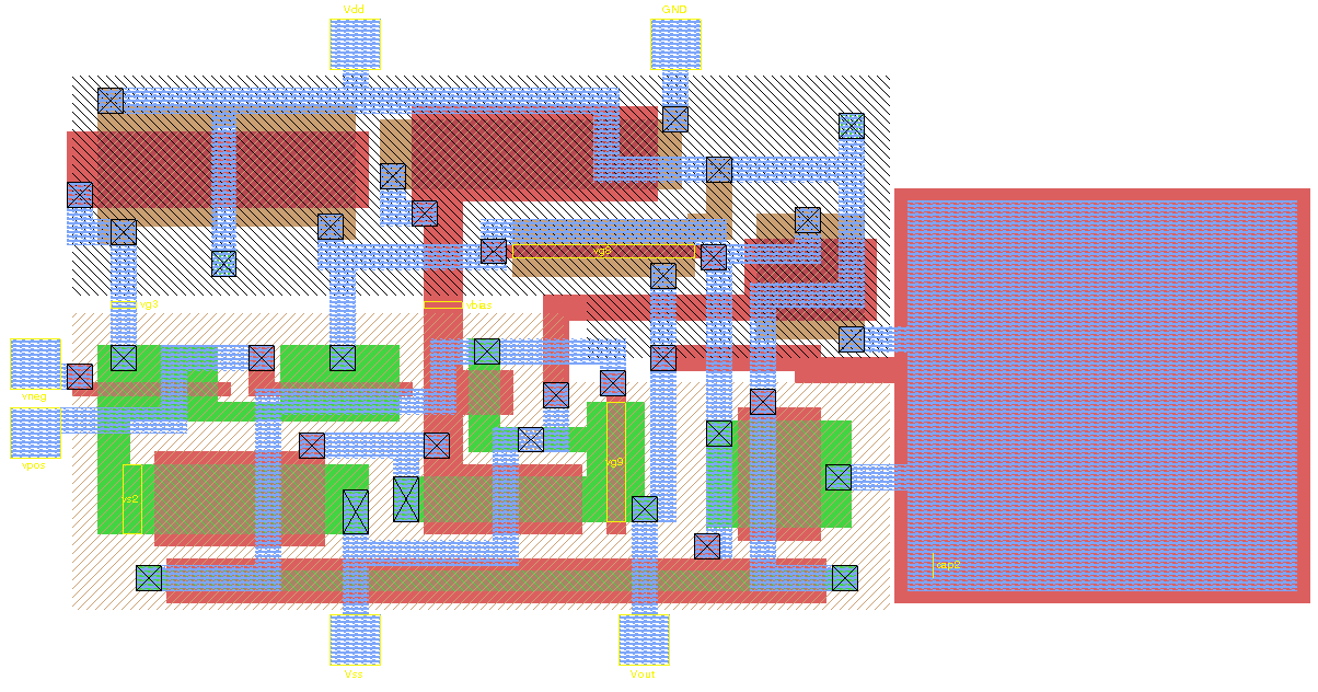
The design of a simple cmos inverter will be presented step by step in order to show the influence of various design rules on the mask structure and on the dimensions. The layout design rules provide a set of guidelines for constructing the various masks needed in the fabrication of integrated circuits. For our purposes there are two primary paths your data will follow once it leaves the cad system. Design rules are consisting of the minimum width and minimum spacing requirements between objects on the different layers.
For emitter and base layout 0 25 µm design rules are used. The rules we need to pay attention to are these. But before we present the options let s go over the basics of mask design.

Layout Design Rules Design Rule Check Drc Vlsi Concepts
Design Of Vlsi Systems Chapter 3

Design Of Vlsi Systems Chapter 3
Layout Rules
Layout Rules
Integrated Circuit Layout Wikipedia

62 Layout Design Rules In Cmos Layout Design In Cmos Rules

Layout Design Rules 2 Introduction Layout Rules Is Also

Sspd Chapter 7 Part 4 Cmos Lay Out Design Rules

Introduction To Layout Design Rules

Design Rule Checking Wikipedia

Stick Diagram Basics 2 Cmos Field Effect Transistor

Design Of Vlsi Systems Chapter 3

Design Of Vlsi Systems Chapter 3
